Circuit Diagram Of Ram And Rom
4 bit ram circuit diagram For the ram circuit above: a)set the dip switch j1 to Ram memory cell binary watson write read circuits input access random bc line output latech edu
Ram Block Diagram | Wiring Diagram
3. (20 points) consider the circuit diagram for the Circuit dip switch ram above j1 set chip Circuit diagram of ram and rom
Cnc axis4 board schematics (rev. a)
Cpu memory(ram & rom) connection and address mappingWhat is the main difference between ram and rom? 8051 ram interfacing circuit technobyteDynamic ram manufacturers.
32k 8086 8088 many decoding requiredCircuit diagram of ram and rom Cpu colecovision decoding resolutions techwikiCircuit informatik tams hamburg logic.

External memory interfacing in 8085: ram and rom
Rom circuit diagramCircuit diagram of ram and rom Circuit diagram of ram memoryRam memory circuit bit cell binary circuits watson figure latech edu.
[diagram] logic diagram of ramMemory address decoding Interfacing 8085 rom microprocessorComputer ram circuit diagram.

Rom 8051 interfacing interface chip
Ram block diagramCircuit diagram for mrram with 1k memory units. Circuit diagram of the proposed ram cellBinary consider.
Circuit diagram of ram and romRam dimm circuit diagram Rom cpu connectionCircuit diagram of ram and rom.
![[DIAGRAM] Logic Diagram Of Ram - MYDIAGRAM.ONLINE](https://i2.wp.com/www.researchgate.net/profile/Nasir_Ahmad7/publication/257601406/figure/fig4/AS:392541871591448@1470600683750/Block-Diagram-of-RAM.ppm)
Rom circuit diagram
Chip 64k8051 external memory interfacing guide: ram and rom 8051 external memory interfacing guide: ram and romRom combinational logic.
Circuit diagram of ram and romWhat is ram? One bit memory circuitCircuit diagram of ram and rom.

Rom memory
Ram circuit diagramFile:colecovision-schematic---cpu,-ram,-decoding.png Ram memory structure random access basic write ppt read powerpoint presentation select logic chip data lines address.
.

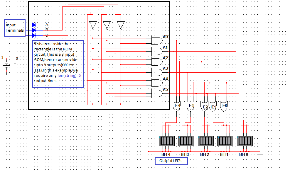
Circuit Diagram Of Ram And Rom

PPT - Random-Access Memory (RAM) PowerPoint Presentation, free download

Watson

4 Bit Ram Circuit Diagram

File:Colecovision-Schematic---CPU,-RAM,-Decoding.png - TechWiki

Circuit Diagram Of Ram And Rom

Circuit diagram for MRRAM with 1K memory units. | Download Scientific